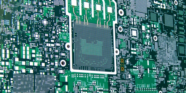
For every advanced electronic device, the PCB Design should meet the advanced technological requirements. These requirements raised the need for the hardware engineers to learn to design a high-speed PCB design. The highly technical devices are designed with a high-speed PCB making the size of the design smaller and compact, handy, more functional, and helps in transmitting data at a faster speed.
But there are certain rules for PCB designing which are very important to adhere to, these rules can be said as the base for designing a PCB. But before you think about designing a high circuit speed board, it is important to understand what “high-speed” means. So, a high speed PCB design is a PCB board that is designed to be operated with high frequencies without hampering the performance of the circuit. There are certain factors to be taken care of while determining the high-speed such as the materials, environment, the circuit, the length of the traces, and the board size. In common terms, it can be assumed that a point with 50MHz speed and above is said to be a high speed design. Jayshree Instruments Pvt Ltd is one of the most suitable PCB design companies in Ahmedabad.
Rules for PCB Designing
A Printed Circuit Board is a designing platform and is one of the flexible parts of an electronic system for original components. The rules for PCB design services in India are today 25 years old and are not changed much since then. The below rules should be practice and kept in mind while designing a PCB:
-
Choose the Right Grid Set
The multi-grid is very effective, but for developing grid basics in PCB design the engineers need to think of it in the early stages of PCB layout, this will help in maximizing the application of the circuit board and avoiding the problems faced in the interval settings. Many devices use multiple package sizes; hence the engineers have to be careful with selecting the products that are conducive to their design. Polygonal copper is applied to the multi-grid circuit boards, but it is not standard as per the single grid and provides a great circuit board life.
-
Keep the Path Short and Direct
This rule is quite common and simple, and this point should be kept in mind at every stage. The PCB path should be short routed and direct one, to give optimum results.
-
Use more Power Layers
The simplest and fastest choice for layers in PCB design software is using the power layer copper. All the large wires are connected, this ensures to provide current with high efficiency and minimum impedance is provided, with also generating adequate ground return paths.
-
Group related components together
The layers in PCB can be single-layered, double-layered and for advanced electronics devices, a multi-layered PCB design is always advisable. The copper traces act as the skeleton of the PCB and the components are the essential organs, with each component having its own desired function. Different components are used for different circuits, and this depends on the electronic device respectively. The commonly used PCB components are LEDs, Transistors, Batteries, Resistors, Inductors, Switches, Diode, and many others.
-
Integrate component values
A designer has to choose the components with lower or higher component values with the same level of performance. By integrating and measuring the value of PCB components within a smaller standard value range, the cost can be reduced and the billing of the materials can also be easier. To be successful with managing the inventory for a longer-term, it is advisable to have PCB products as per the preferred value of the component.
-
Perform Design Rule Check
While carrying out a PCB designing process, it is advisable to carry out the Design Rule Check function frequently, especially for PCB software operating in a complex design environment. Checking the performance throughout the designing process can help in saving time.
-
Use Screen Printing flexibly
A PCB screen printing marks the important information on the PCB board which is can be used by the installers, equipment debuggers, test engineers or service engineers, or the manufacturers in the future for their reference. The marks are not only related to test point labels or mark clear functions, but also the direction of the connectors and components too, many times the comments may be printed on the lower surface of the PCB components. The full application of the screen printing process on the lower and upper surfaces of PCB can help in smoothening the production process and also help in reducing the repetition of work.
-
Must select Decoupling Capacitors
The decoupling capacitors used are durable and not much expensive, so you can spend whole-heartedly assembling the capacitors. It is also advisable to optimize the PCB design without avoiding decoupling the power as per their limit values. And to keep your inventory tidy always use the standard value range and follow the DRC process.
-
Generate and Verify PCB Manufacturing Process
The last and final rule is to check whether the PCB manufacturing parameters are adhered to or not. The PCB manufacturers are quite supportive and will verify the same for you to avoid any further confusion, but you can also check the same Gerber file and check whether PCB design standards are maintained or not. This will help in rectifying the errors and avoiding any other losses too.
Jayshree Instruments Pvt. Ltd serves all the technical needs of their clients and provides the best electrical systems, be it any type of cable assembly manufacturing needed. One can also customize the electric cable assemblies as per their needs and requirements. You can further contact us more details on Jayshree Instruments Pvt. Ltd.

Recent Comments