Established in 2001, Jayshree Instruments provides PCB assembly services which is considered as one of the most challenging aspects of electronic product design. Our mission is to serve the design, engineering and contract manufacturing outcomes as per the customer’s needs. We assure to give life to their choice of products as expected. The process of PCB assembly involves materials of the best quality along with best of technology and precise designing. With PCB circuit board assembly, we also provide other electronic manufacturing services.
Find some information about world-class PCB services:
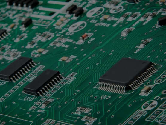
The PCB assembly has numerous steps which includes surface mount technology (SMT) and through hole technology. SMT is a process where the electrical components are mounted on the surface of a PCB. In the SMT PCB assembly process, the printer circuit board consists of the solder paste on the connection pads along with the components, which are then reflowed in a furnace to melt the solder paste. It then forms connections in the electrical and mechanical components leading to the PCB.
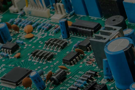
In the through-hole PCB assembly process, the component leads are used onto the board and the leads are joined via the Dip soldering process. A few SMT components can be used on the lower side of the board and can be joined by the wave soldering method.

One-stop fabrication and assembly

Parts sourcing

Comprehensive quality assurance

Professional engineering team

High efficiency with competitive price ranges
Jayshree Instruments is an Ahmedabad based company offering the most authentic and adaptable PCB assembly manufacturer from India. We promise flawless and value for money production of various kinds of complicated and heavy PCB assembly from India.
Get A Quote Now
SURFACE MOUNT ASSEMBLY – SMT
SMT is a process where the electrical components are directly mounted on the surface of a PCB. In the SMT PCB assembly process, the printer circuit board consists of the solder paste on the connection pads along with the components, which are then reflowed in a furnace to melt the solder paste. It then forms connections in the electrical and mechanical components leading to PCB.
- Tin Lead or RoHS Compliant
- High Speed Pick and Place
- High Volume Production
- Single and Double Sided SMT assembly
- Min. pitch 0.25mm placement
- SMD packages down to 0402
- Largest component: QFP & BGA to 32 x 32mm
- Multi-Zone Convection Reflow Ovens
- Semi-Automatic Screen Printing
- Max PCB panel size: 1500mm L x 400mm W


THROUGH HOLE ASSEMBLY
Jayshree instruments, one of the best PCB assembly companies in Gujarat offer a variety of services and capabilities that add value to the product. The operations of Through Hole PCB Assembly includes the art component prep equipment. The components used in the through hole PCB assembly process are lead free RoHS compliant.
Our PCB through hole technology capabilities include insertion which offers an outcome of excellent product quality assuring the project is completed with utmost care by our experienced and trusted employees.
To keep the product quality consistent we follow the first piece process which is overlooked by our highly skilled and experienced operators along with the engineering support team who monitor each and every project minutely to ensure the best results to our customers.
CONFORMAL COATING
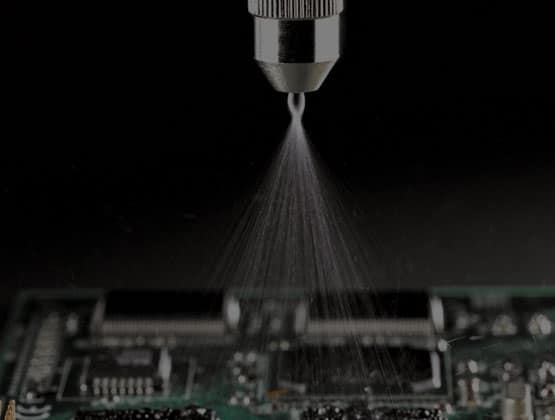
Conformal coating is a coasting done for protection which conforms to the circuit board topology. The coasting protects the electronic circuits from harsh surroundings that may have high humidity, airborne contaminants and changing temperatures. Jayshree Instruments offer specific bulk conformal coating services like sprayings and spray coating with component masking for PCB Assembly and numerous electronic devices.

Other PCB Services
Jayshree instruments is one of the best PCB manufacturers in India offering PCB assembly services with best of accuracy and quality. Here are some of the other PCB services:
INDUSTRIES
Jayshree Instruments provide best quality and performance oriented PCB’s, considering the time limit and budget constraints. We assure end to end PCB manufacturing services to numerous industries. Being in this business since a really long time we do understand your requirements related to your industry. And this is why we are a competition to many when it is about delivering the perfect PCB. Our team is ready to create the perfect PCB for any kind of industry be it for medical equipment or for command and control systems for military applications. Usually there are no common solutions of different kind of industries and so we provide custom PCB manufacturing services focusing on all complex requirements considering your timeframe, specifications and budget.
MEDICAL
Medical industry requires electronic equipment with a high level of accuracy and clarity ensuring long term usage. PCB manufacturers for the medical industry need the best quality and sanitary control. Jayshree instruments is one of the best PCB manufacturer in India offering medical PCB assembly services which can be used efficiently and are safe. To serve the best treatment to the patients it is important to keep the medical equipment in the best possible condition. Our team assures technical assistance at reasonable cost.
MILITARY
Military equipment’s need to be sturdy and accurate enough, as they need to be operated in hostile working spaces. Their equipment should also be adaptable enough which can be updated based on the upcoming technologies. One of the most integral parts of these equipments are the PCB’s. Print circuit boards for military equipments are created in a way that they can be operated in harsh working situations. We serve such PCB’s in variety of designs, materials and composites to fulfill tough requirements of military and defense systems.
CONSUMER ELECTRONICS
The requirement of advanced electronic devices is much in demand. PCB assembly services have grown parallel to the rapidly developing demand of consumer electronics. And now numerous electronic devices depend on well-crafted and assembled PCB’s. With the appropriate PCB components, all electronic devices can be operated easily. Our team follows the client requirements while assembling the PCB.
MECHANICAL
Mechanical engineering is the oldest engineering discipline and it is growing and has become advances over all these years. In today’s world it includes automation in product, machining, manufacturing and tooling. Mechanical devices have helped us simplify lives and have enhanced productivity and pace of life. These mechanical devices are utilized in numerous industrial as well as consumer applications. Jayshree Instruments offers a blend of technology and engineering skills to provide the quality products with the requested requirements.
Why work with us?
Jayshree Instruments assures optimal PCB services to satisfy your company’s PCB assembly requirements. We do offer different materials from which you can make your choice along with the technology options. We promise start to end solutions satisfying all your requirements. Know more about PCB assembly services we provide including high-quality assembly services.
ONE STOP FABRICATION AND ASSEMBLY
With years of experience in the industry of PCB fabrication and assembly, we create high-quality PCB’s which are cost effective and authentic.
MULTIPLE SERVICES LIKE SMT, THT, MIXED ASSEMBLY, OP ETC.
We offer a variety of print circuit boards like surface mount PCB assembly, through hole PCB assembly, mixed assembly, conformal coating etc.
FLEXIBLE VOLUME ASSEMBLY ALTERNATIVES
Jayshree Instruments serve assembly alternatives with flexible volume options like prototypes, full turnkey PCB assembly, low volume and high volume.
PARTS SOURCING
We are well connected with distributors and manufacturers creating authorized electronic components. So we make sure you get genuine and good quality equipment. All these parts go through the best quality inspection.
COMPREHENSIVE QUALITY ASSURANCE
For us quality control is very important, and so for visual inspection to AOI and x-ray inspection, the quality and functionality is tested aggressively.
HIGH EFFICIENCY, LOW COST
At reasonable cost you will get the best quality as we have a team of experienced and skilled experts taking care of your minutest requirements.
PROFESSIONAL ENGINEERING TEAM
Our team of dedicated and qualified engineers are the reason behind all our successful projects. They make sure to keep an eye on optimizing designs, quality and consideration of timeline as well as budget.
PROCESS OF PRINT CIRCUIT BOARD ASSEMBLY
There is a before and after procedure for the PCB Assembly that includes particular steps. The phases leading up to the assembling process are explained here:
STEP 1: Solder Paste Stenciling
The application of solder paste to the circuit board is the first stage in PCB assembly. This procedure is carried out similarly to screen-printing a shirt, except instead of using a mask, a thin stainless steel stencil is used here and adhered to the PCB. Assemblers take the step of only applying solder paste to certain PCB regions. The components of the real PCB settle in this region.
If it is a professional PCBA line, the PCB and stencil are held in place by a mechanical stand. Then, using an applicator, a certain quantity of solder paste is put where it is needed. The paste is then applied uniformly to the open space on the stencil by the machine, which keeps doing so. When this phase is complete, the stencil may be taken off, and the solder paste will remain where it was supposed to.
STEP 2: Pick and Place
The PCBA process then proceeds to the pick and place machine, where a robotic device attaches surface mount components to the prepared PCB, following the first stage. SMDs then inspect PCBs for any components without connectors. The surface mount components, also known as SMDs, are then soldered onto the circuit board in a subsequent step.
With a pair of tweezers, the operation may be completed manually, requiring the assembler to choose and position each component by hand. But today, among PCB makers, this phase is often carried out by an automated procedure. The procedure changed from being manual to automation since machines are usually more accurate and reliable. Machines can operate for extended periods of time without experiencing difficulties like eye strain or weariness.
STEP 3: Reflow soldering
The necessity for the surface mount components and solder paste to be together and in position means that the solder paste must harden in order to hold the components to the board.
This approach may be applied in PCB assembly through the “reflow” stage. The PCB board is carried to the conveyor belt after the pick and place process, where it passes through a massive reflow oven that resembles a commercial pizza oven. A number of heaters in the oven heat the board to a temperature of 480 degrees Fahrenheit (250 degrees Celsius), which is high enough to melt the solder in the solder paste. The solder begins to melt as it enters the oven and continues as it moves through the succession of cooled heaters. As a result, the molten solder may cool down under regulated conditions and take on a solid shape.
The SMDs and PCB are kept linked by using a fixed solder junction that is produced by this procedure. Many PCBAs require specific care during the reflow process, particularly when two-sided PCB Assembly is involved.
STEP 4: Inspection and Quality control
The board has to be checked for functionality following the reflow procedure and after the surface mount components have been soldered in place. There are occasions when disturbances during the reflow process result in a poor connection or no connection at all. Shorts are another negative effect of this movement, as misplaced components frequently link circuits that are not intended to be connected. Cross-checking such mistakes and misalignments is one of several inspection techniques.
– Manual checks:
Apart from the upcoming latest trends of automated and smart manufacturing, self and manual checks are still trusted in the PCB Assembly process. For smaller lots, an in-person analysis by an experienced designer is an effective method to inspect the quality of a PCB post the reflow steps. Although, this process tends to become increasingly impractical and uncertain as the figure of inspected boards increases. Looking at such nominal components for more than an hour may lead to optical fatigue which leads to less accurate inspections.
STEP 5: Through-Hole Component Insertion
The kind of board under PCBA may have several types of components in addition to the usual SMDs. Components with through-hole plating may also be included in this. PTH refers to a PCB hole that is plated through the board.
These holes are utilized by the PCB components to transmit signals from one side of the board to the other. Soldering paste would not be helpful in these situations since it will just flow through the hole without having an opportunity to attach. PTH components require more specialized and advanced soldering techniques, such as hand soldering and wave soldering, as a replacement for soldering paste in the subsequent PCB assembly process.
The PCB can go to the final inspection when this phase is finished, or it can go back and repeat them if more parts need to be added.
STEP 6: Final Inspection and Functional Test
The final examination of the PCBs functioning takes place after the soldering phase of the PCBA process. The “functional test” is another name for this kind of test. The PCB is put through its paces in this test, simulating the conditions in which it will typically function. During this examination, simulated signals and power are sent via the PCBs. Additionally, the testers keep track of the electrical properties of the PCB.


