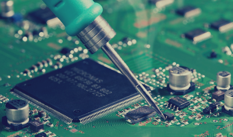
No matter how much experience a PCB Design Engineer has in designing and creating electronics out on a circuit board, you still need to be aware of the detailed design that could affect PCB manufacturing. Many PCB designers experience difficulties while setting up hardware designs for the smooth and reliable working of the circuit board manufacturing. Many times the PCB designers might not have direct access to the complexities of PCB production. This might cause issues with components and design which might lead to manufacturing problems for PCB design. The electronic manufacturing company can also partner with Quality CMs who have a great level of experience from different industries and can help to resolve these issues.
Jayshree Instruments Pvt Ltd is an electronic manufacturing company in Ahmedabad with a higher level of expertise in the manufacturing, development, and testing of PCB circuit boards.
List of PCB Design Manufacturing Problems
Many PCB manufacturing problems can affect the working of the electronic circuit board, and the designer should be well aware of these issues. Let’s have a look at the PCB Manufacturing Problems in detail listed below:
- PCB Materials
- Components
- Starved Thermals
- Copper too close to the board edge
- Missing solder mask between pads
- Tombstoning
-
PCB Materials
The companies dealing with electronic manufacturing services have to be very cautious about the PCB materials. The materials used to fabricate a PCB varies for specific circuits, and circuits require certain materials such as FR-4, MCPCB, and so on. The board layer stacks require a different level of materials. So for best signal integrity performance, it is suggestible to use these materials only. It is also necessary to assess the operating environments, whether it is suitable for the materials or not. This helps to reduce the cost too.
-
Components
One of the major PCB design issues to be considered is the usage of PCB components. It might happen that the designer is using the same old surface mount components or PCB components for years and years. And, they might not realise that the effectiveness of the components can change with time. So the designers must be updated in terms of selecting the components, this will help in a shorter lead time.
-
Starved Thermals
The thermal relief traces connecting the pad should be nicely connected to the associated lane, if the connection is not proper, the problem of starved thermals can occur. One of the basic PCB Design rule checks is to examine the spacing between vias, this might lead to interruption between the attached thermal traces and can also affect the connection of the assigned copper pours. This is most commonly observed when multiple vias are placed close to each other.
-
Copper too close to the board edge
One of the design rule checks involved with PCB layout design service is the proper placing of copper layers. As the proximity of copper to the edge of a board may lead to the shortening of the layers together when the board is cut into specific sizes during the PCB fabrication process. It is advisable to identify this error using the Design Rule Check feature (DRC feature) that is available in PCB design software. A PCB fabricator that can conduct a Design for Manufacturability check can also help to identify this issue.
-
Missing solder mask between pads
It might also happen that there can be no solder mask between pins in small pin pitch devices that are close spaces. This can happen due to the standard design settings of the PCB Assembly. The missing solder mask between the pads can form bridges when the pin-pitched component is combined with the circuit board.
Jayshree Instruments Pvt. Ltd. has been one of the professional PCB design companies in Ahmedabad for years now, who are also capable of avoiding missing solder mask between pads.
-
Tombstoning
With the help of the reflow process, small passive surface mount components are soldered to a PCB assembly by lifting it on one end and tombstone it. This process of tombstoning can increase the production costs and functioning of the PCB. Imbalanced thermal relief and incorrect landing patterns can be the source of tombstoning. DFM check is the best way to know about the problem of tombstoning.
There are many other PCB manufacturing problems that a PCB designer might come across such as insufficient annular ring, silvers, and the issue of acid traps. The PCB designer needs to rectify these errors through the DFM check or DRC check method.
Jayshree Instruments Pvt. Ltd. has been a custom PCB for years now. We have experience dealing with all types of PCB assembly boards. You can further visit our website Jayshree Instruments Pvt Ltd for further details.

Recent Comments